
In-house SEM Services
NEI Corporation is proud to expand its analytical services to include in-house Scanning Electron Microscopy (SEM). Our cutting-edge SEM capabilities provide unparalleled microscopic imaging and analysis for a wide range of materials and applications.
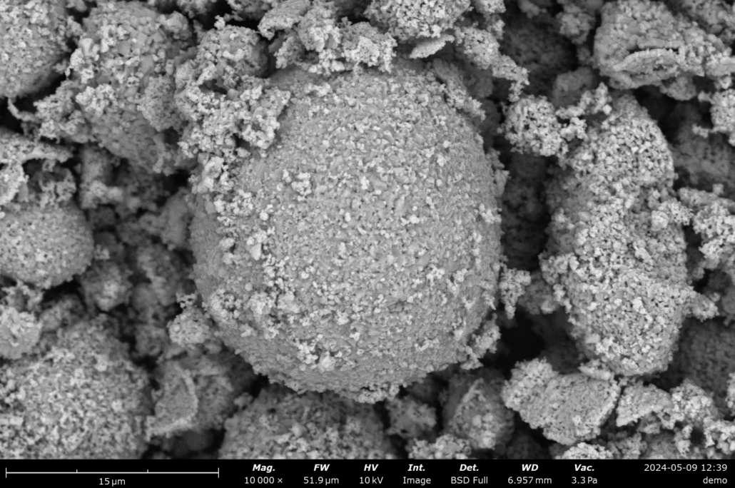
Powders
Surface of Lithium-ion anode powder particle
(shown at 10,000x magnification)
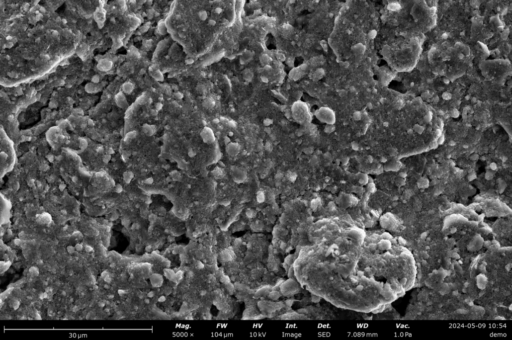
Electrode Surface
Top surface of a Li-ion battery electrode sheet
(shown at 5,000x magnification)

Coating Cross-Section
Cross-section of a protective surface coating
(shown at 10,000x magnification)
Why Choose NEI for Your SEM Needs?
NEI Corporation’s commitment to excellence extends to our SEM services. Our advanced equipment and expert team deliver reliable, accurate, and timely results. SEM imaging can be provided as a standalone service, or it can be integrated with other characterization or R&D services that we offer.
- High-Resolution Imaging: Our advanced SEM systems deliver exceptional image quality, revealing intricate details at the nanoscale.
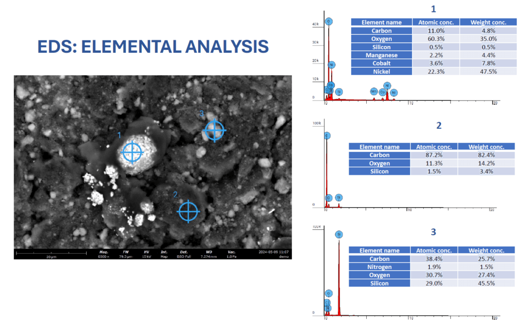
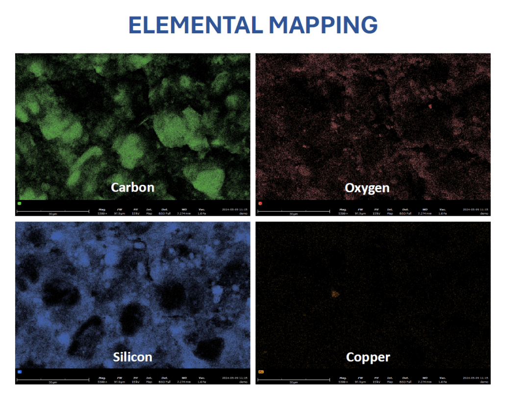
- Elemental Analysis: Determine the elemental composition of a sample using Energy Dispersive X-ray Spectroscopy (EDS)
- Versatile Analysis: Explore a wide range of materials, from metals and polymers to ceramics and composites.
- Expert Interpretation: Our experienced scientists can provide in-depth analysis and interpretation of SEM data.
- Tailored Solutions: Benefit from our customized SEM services to address your specific research or quality control requirements.
Select a tab below to learn more about our available SEM services or Request a Quote.
High-Resolution Imaging
See Your Materials Like Never Before
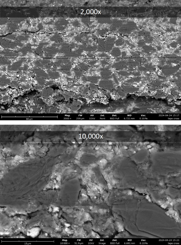
Cross-section of a cast electrode sheet shown at 2,000 and 10,000 magnification
High-resolution imaging through Scanning Electron Microscopy (SEM) gives you the ability to visualize the incredibly fine details of a sample’s surface topography. Our SEM equipment has both a Backscattered Electron Detector (BSD) and a Secondary Electron Detector (SED), which can be configured to readily identify different phases present in a sample and provide crisp and high-resolution surface-sensitive imaging. This level of detail allows for:
- Observation of nanoscale features: Revealing structures, defects, and particles that are invisible to traditional microscopes.
- Precise measurements: Determining the size, shape, and distribution of nanoscale components with high accuracy.
- Detailed surface characterization: Understanding the surface roughness, texture, and topography of materials.
Materials Science Applications include:
- Battery: High-resolution imaging of battery materials offers invaluable insights for optimizing performance, longevity, and safety. By visualizing the material’s microstructure, researchers and engineers can understand degradation mechanisms, optimize material design, improve quality control, and even accelerate battery development.
- Coatings: SEM offers a wealth of information crucial for the coatings industry. By visualizing the coating’s microstructure at the nanoscale, manufacturers can accelerate coating development by analyzing failure modes to improve quality control and optimize coating performance.
Available Magnifications:
Our SEM can obtain images up to 100,000 times magnification and resolution smaller than 10 nm.
SEM Elemental Analysis
EDS Image Samples

Process Overview
Get a Quote